ASR5822S Datasheet
Introduction
About This Document
This document introduces the specifications of ASR5822S chip (Wi-Fi 4+BLE 5.1 Combo SoC).
Intended Readers
This document is mainly for engineers who use this chip to develop their own platform and products, for instance:
PCB Hardware Development Engineer
Software Engineer
Technical Support Engineer
Included Chip Models
The product models corresponding to this document are as follows.
Model |
Protocol |
Core |
SiP Flash |
Operating Modes |
|---|---|---|---|---|
ASR5822S |
Wi-Fi 4 BLE 5.1 SIG Mesh v1.0.x |
Arm China STAR-MC1 Processor |
2 MB |
11 b/g/n: Support Station/SoftAP/Sniffer Support IoT mode/SDIO mode BLE 5.1: Support multiple-speed modes Support Mesh Support AOA/AOD Pass BQB 5.2 certification |
Copyright Notice
© 2023 ASR Microelectronics Co., Ltd. All rights reserved. No part of this document can be reproduced, transmitted, transcribed, stored, or translated into any languages in any form or by any means without the written permission of ASR Microelectronics Co., Ltd.
Trademark Statement
ASR and ASR Microelectronics Co., Ltd. are trademarks of ASR Microelectronics Co., Ltd.
Other trade names, trademarks and registered trademarks mentioned in this document are property of their respective owners.
Electrostatic Discharge (ESD) Warning
This product can be damaged by Electrostatic Discharge (ESD). When handling with this device, the people should be very careful to conduct the ESD protection to avoid any device damage caused by ESD event.
Disclaimer
ASR do not give any warranty of any kind and may make improvements and/or changes in this document or in the product described in this document at any time.
This document is only used as a guide, and no contents in the document constitute any form of warranty. Information in this document is subject to change without notice.
All liability, including liability for infringement of any proprietary rights caused by using the information in this document is disclaimed.
ASR Microelectronics Co., Ltd.
Address: 9F, Building 10, No. 399 Keyuan Road, Zhangjiang High-tech Park, Pudong New Area, Shanghai, 201203, China
Homepage: http://www.asrmicro.com/
Revision History
Date |
Version |
Release Notes |
|---|---|---|
2023.09 |
V1.7.1 |
Updated Table 2-5. |
1. Overview
1.1 General
ASR5822S is a highly integrated, high performance, and low cost System-on-Chip (SoC) which supports both 1x1 IEEE 802.11 b/g/n and Bluetooth 5.1 Low Energy (BLE) for the Internet of Things (IoT). The ASR5822S integrates RF transceiver, 802.11 PHY+MAC, BLE PHY+MAC, Arm China STAR-MC1 Processor, advanced peripheral interfaces, Real Time Counter (RTC) and power management circuits. The integrated RF and analog circuit incorporate T/R switch, RF balun, power amplifier, low-noise amplifier, and entire power management modules. Therefore, the ASR5822S provides a small form-factor solution with minimal external components for the IoT applications, such as smart lighting, security, remote control, appliances and more.
The chip can perform either as a standalone IoT application with Supplicant/HostAP/Sniffer mode or as a slave with SDIO interface.
Solution Highlights:
Fully Integrated Power Management Circuits
The chip includes an on-chip DCDC associated with LDOs to provide noise isolated power supplies for digital and analog modules. The DCDC has a single, wide-range (3.3~5 V) supply input and dual outputs (1.2 V, 1.8 V) to extremely minimize Bill of Material (BoM). Moreover, the chip provides two UART interfaces that can follow the DCDC supply to adjust interface voltage range from 3.3 V to 5 V. And a UART interface can support ESD HBM larger than 6 KV, which can save the ESD diode device to reduce the module cost further.
WLAN and BLE Co-existence
ASR5822S has an excellent co-existence performance. The chip supports network configuration via BLE and BLE Mesh, which can provide multiple development capacities for the customers.
Entire Security System
A completed security infrastructure, including AES/RSA/ECC crypto engine, hash engine and True Random Generator (TRNG), is also integrated. ASR5822S can provide a comprehensive security solution as Security Boot flow, Flash Image Protection and dynamic encryption/decryption for customer data.
Entire Software Solution
ASR5822S provides an entire software solution, such as RTOS/TCPIP/SSL/MQTT/ Wi-Fi/AT and more. The customers just need to simply develop applications and then put them into the market.
In pass through application scenario, the customers can control ASR5822S with AT command through UART interface without any code developing in ASR5822S. In master-control application scenario, the customers just need to focus on their own application developing, with the OS/communication layer/Security already supported in ASR5822S SDK.
1.2 Features
Power Management Unit (PMU)
Integrated DCDC and LDO, no need of off-chip PMU device
Support single supply input, range from 3 V ~ 5.5 V
IEEE 802.11 Features
Integrated Power Amplifier (PA) with internal power detector and closed loop power calibration
Integrated T/R switch and RF balun, no need of off-chip matching network
Support 802.11 b/g/n compatible WLAN
Support 802.11e QoS enhancement (WMM)
Support 802.11i (WPA/WPA2 PSK/WPA3 personal), Open/WEP/TKIP/CCMP
Support power saving mechanism
BLE Features
AOA/AOD direct finding
2 x speed with 2 M bps support
4 x distance with 125 K bps data rate in long range mode
8 x advertising capacity
Better frequency hopping
BLE SIG Mesh: Relay/Proxy/Low power/Friend features
SoC Features
Arm China STAR-MC1 Processor associated with 24 KB cache
352 KB RAM for Instruction and Data
64 KB ROM is integrated
4K-bit OTP is integrated
MCU Core Clock: 160 MHz
XTAL Clock: 26/40 MHz
Support eXecute-in-Place (XiP) on flash and external SPI flash
External SPI NOR Flash is supported up to 256 MB
Support Category: GigaDevice, WB and XTX
Support OTA
Security
Hardware Security Engine
AES/RSA/ECC/MAC/HMAC/SHA1/SHA-224/SHA256/SHA512/D-H library
True Random Number Generator (TRNG)/PRNG
Flash Image Integrated Encryption/Decryption
Dynamic Encryption/Decryption for Customer Data
Integrated eFuse OTP
Peripherals
UART/SPI/I2C/PWM/I2S/Timer
PSRAM controller
Generic ADC x8 Channels
Watchdog
RTC
1.3 Block Diagram

1.4 Applications
Smart Plugs and Lights
Wearable Electronics
Home Appliances
Home Automation
Mesh Network
Industrial Wireless Control
Sensor Networks
1.5 Part Number Information
The following table shows ASR5822S part number information.
Part Number |
Pin Number |
Package Type |
Pitch |
SiP Flash |
Thickness |
Comments |
|---|---|---|---|---|---|---|
ASR5822S |
40 |
QFN 5 mm x 5 mm |
0.4 mm |
Yes |
0.85 mm |
2. System Function Descriptions
2.1 PMU
ASR5822S can support 3.3 V ~ 5 V single power supply, which can come from a battery or a DC-DC convertor or an AC-DC convertor directly. There is no need of any other off-chip DCDC or LDO device. The PMU consists of Always-ON (AON) control logic, RTC circuits, DCDC, and LDOs. All these circuits have characters of low noise and low quiescent current performances.
DCDC is powered by single power supply and it generates two BUCK voltages of 1.2 V and 1.8 V. 1.2 V BUCK is supply for Digital LDO (DLDO). 1.8 V BUCK is supply for all Analog LDOs (ALDO). The LDO33 has 3.3 V output that provides supply for DVDD IO, RTC LDO (RLDO) and 3.3 V analog circuits.
ASR5822S’s PMU provides several low power modes: modem sleep, light sleep and deep sleep. These modes meet different application requirements.
The chip’s power grid and power-on sequence are described as follows:


Symbol |
Parameter |
Typical |
Maximum |
Unit |
|---|---|---|---|---|
T_33 |
RVDD33_LDO rising time |
200 |
600 |
us |
T_11aon |
VDD11_AON rising time |
100 |
500 |
us |
T_wait |
AVDD18/AVDD12 wait time |
350 |
800 |
us |
T_18 |
AVDD18_xxxrising time |
150 |
1000 |
us |
T_12 |
AVDD12_DIGLDO rising time |
150 |
1000 |
us |
T_wait_11core |
VDD11_CORE wait time |
60 |
150 |
us |
T_11core |
VDD11_CORE rising time |
150 |
1000 |
us |
2.2 Clock
ASR5822S supports 26 M or 40 M XO frequency to generate all high performance clock signals in on-chip RF/Analog PLL. In RTC, circuits support one low-power clock source, the RC Oscillator (RCO). The customer can use RCO as RTC reference clock to save the BoM. The RCO frequency can be auto-calibrated on chip.
2.3 CPU Functions
2.3.1 Introduction
ASR5822S includes an integrated Arm China STAR-MC1 Processor with internal RAM and ROM. The high-performance Arm China STAR-MC1 Processor provides a low-cost platform that meets the needs of minimal memory implementation, reduced pin count, and low power consumption, while delivering outstanding computational performance and exceptional system response to interrupts. The Arm China STAR-MC1 Processor includes instruction and data cache, and floating point arithmetic functionality.
2.3.2 Features
The inside Arm China STAR-MC1 core has Floating Point Unit (FPU), Cache Controller and Memory Protection Unit (MPU) and with the following features:
Arm V8-M architecture based instruction set optimized for embedded applications
Tightly Coupled Memory (TCM) interface to achieve higher MIPS
A Nested Vectored Interrupt Controller (NVIC) closely integrated with the processor core to achieve low latency interrupt processing
A low-cost debug solution featuring with serial wire debug port (SW-DP)
Multiple high-performance bus interfaces
2.4 Memory
2.4.1 ROM
The internal 64 KB ROM of ASR5822S device is at address 0x0000_0000 of the device memory. It stored the boot rom image, mainly used to program the flash image/take secure boot function/take non-secure boot function according to the Mode Selection.
2.4.2 SRAM
ASR5822S family provides up to 352 KB of on-chip SRAM. The internal RAM is not only used for code and data memory, but also used for shared memory for Wi-Fi/BLE packet buffer. It can be configured by software remap register. Internal RAM is capable of selective retention in power-saving mode.
2.4.3 FLASH
ASR5822S provides 2 MB of System-in-Package (SiP) QSPI Flash with hardware encryption and flash remapping functions to protect developers’ programs and data. ASR5822S supports up to external 256 MB QSPI flash or SRAM devices for user applications.
The Arm China STAR-MC1 Processor can access the QSPI flash or SRAM through high-speed caches.
2.4.4 One-time Programmable Memory
ASR5822S provides 4K-bit One-Time Programmable (OTP) memory.
Hardware configuration parameters including Flash-Encryption may be stored in first internal 2K-bit OTP memory, which is read by system software after device reset. In addition, customer-specific parameters can be stored, depending on the specific board design in reserved 2K-bit OTP memory.
2.4.5 Memory Mapping
The following table describes the various MCU peripherals and how they are mapped to the processor memory.
Description |
Start Address |
End Address |
|---|---|---|
ROM |
0x0000_0000 |
0x0000_FFFF |
ITCM |
0x0008_0000 |
0x0008_7FFF |
FLASH |
0x1000_0000 |
0x17FF_FFFF |
DTCM |
0x20FD_0000 |
0x20FF_FFFF |
System SRAM |
0x2100_0000 |
0x2101_FFFF |
External Flash/SRAM |
0x3000_0000 |
0x3FFF_FFFF |
SYS_CON |
0x4000_0000 |
0x4000_0FFF |
GPIO0 |
0x4000_1000 |
0x4000_1FFF |
GPIO1 |
0x4000_2000 |
0x4000_2FFF |
QSPI |
0x4000_3000 |
0x4000_3FFF |
System DMA |
0x4000_4000 |
0x4000_4FFF |
OTP |
0x4000_5000 |
0x4000_5FFF |
SDIO |
0x4000_7000 |
0x4000_7FFF |
RETENTION Memory |
0x4000_8000 |
0x4000_8FFF |
PSRAM Controller |
0x4000_A000 |
0x4000_AFFF |
CYPT310 |
0x4000_D000 |
0x4000_DFFF |
WDT |
0x4008_0000 |
0x4008_0FFF |
UART0 |
0x4008_1000 |
0x4008_1FFF |
UART1 |
0x4008_2000 |
0x4008_2FFF |
UART2 |
0x4008_3000 |
0x4008_3FFF |
SPI0 |
0x4008_4000 |
0x4008_4FFF |
SPI1 |
0x4008_5000 |
0x4008_5FFF |
SPI2 |
0x4008_6000 |
0x4008_6FFF |
TIMER |
0x4008_7000 |
0x4008_7FFF |
PWM |
0x4008_8000 |
0x4008_8FFF |
ADC |
0x4008_9000 |
0x4008_9FFF |
I2C0 |
0x4008_A000 |
0x4008_AFFF |
I2C1 |
0x4008_B000 |
0x4008_BFFF |
I2S |
0x4008_F000 |
0x4008_FFFF |
2.5 Peripherals
The following table gives a summary of all peripherals of ASR5822S.
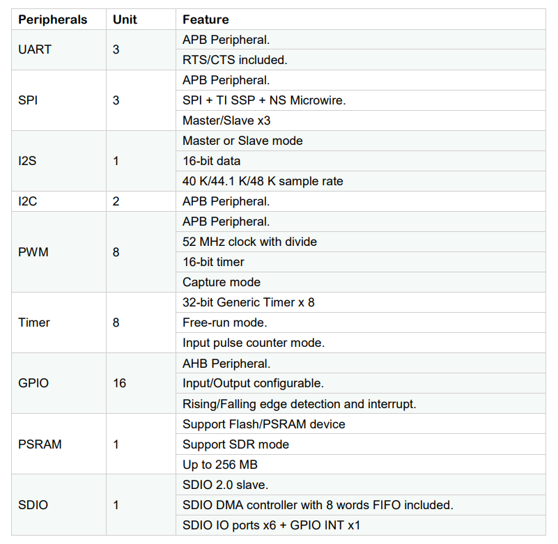
2.5.1 PIN MUX
All GPIO can be reconfigured via software control. The PIN MUX table is shown as follows.
Num. |
Pin Name |
GPIO Func=0 |
GPIO Func=1 |
GPIO Func=2 |
GPIO Func=3 |
|---|---|---|---|---|---|
1 |
DIG_PAD0 |
GPIO0 |
UART0_TXD |
SWC |
SPI1_CSN |
2 |
DIG_PAD1 |
GPIO1 |
UART0_RXD |
SWD |
SPI1_SCK |
3 |
DIG_PAD2 |
GPIO2 |
UART1_TXD |
UART1_TXD |
SPI1_DI |
4 |
DIG_PAD3 |
GPIO3 |
UART1_RXD |
UART1_RXD |
SPI1_DO |
5 |
DIG_PAD4 |
SWC |
GPIO4 |
SDIO_CMD |
UART0_TXD |
6 |
DIG_PAD5 |
SWD |
GPIO5 |
SDIO_CLK |
UART0_RXD |
7 |
DIG_PAD6 |
GPIO6 |
SPI0_CSN |
SDIO_DATA0 |
UART0_CTS |
8 |
DIG_PAD7 |
GPIO7 |
SPI0_SCK |
SDIO_DATA1 |
UART0_RTS |
9 |
DIG_PAD8 |
GPIO8 |
SPI0_TX |
SDIO_DATA2 |
I2C1_SCL |
10 |
DIG_PAD9 |
GPIO9 |
SPI0_RX |
SDIO_DATA3 |
I2C1_SDA |
11 |
DIG_PAD10 |
MODE_SEL3 |
PWM1 |
GPIO10 |
UART2_CTS |
12 |
DIG_PAD11 |
GPIO11 |
PWM3 |
SDIO_INT |
UART2_RTS |
13 |
DIG_PAD12 |
GPIO12 |
GPIO12 |
SPI2_CSN |
UART2_TXD |
14 |
DIG_PAD13 |
GPIO13 |
GPIO13 |
SPI2_DO |
UART2_RXD |
15 |
DIG_PAD14 |
STRAP/SEL1 |
PWM0 |
SPI2_SCK |
UART1_CTS |
16 |
DIG_PAD15 |
STRAP/SEL2 |
PWM2 |
SPI2_DI |
UART1_RTS |
Num. |
Pin Name |
GPIO Func=4 |
GPIO Func=5 |
GPIO Func=6 |
GPIO Func=7 |
ADC Mux |
|---|---|---|---|---|---|---|
1 |
DIG_PAD0 |
PWM5 |
N/A |
|||
2 |
DIG_PAD1 |
PWM7 |
N/A |
|||
3 |
DIG_PAD2 |
I2C0_SCL |
N/A |
|||
4 |
DIG_PAD3 |
I2C0_SDA |
N/A |
|||
5 |
DIG_PAD4 |
PWM0 |
N/A |
PSRAM_SIO3 |
ADC0 |
|
6 |
DIG_PAD5 |
PWM2 |
N/A |
PSRAM_SIO2 |
ADC1 |
|
7 |
DIG_PAD6 |
PWM4 |
N/A |
PSRAM_SCK |
ADC2 |
|
8 |
DIG_PAD7 |
PWM6 |
N/A |
I2S_MCLK |
PSRAM_SIO1 |
ADC3 |
9 |
DIG_PAD8 |
UART1_TXD |
N/A |
I2S_SCLK |
PSRAM_SIO0 |
ADC4 |
10 |
DIG_PAD9 |
UART1_RXD |
N/A |
I2S_LRCLK |
PSRAM_CSN |
ADC5 |
11 |
DIG_PAD10 |
SPI2_SCK |
N/A |
I2S_DO |
ADC6 |
|
12 |
DIG_PAD11 |
SPI2_DI |
N/A |
I2S_DI |
ADC7 |
|
13 |
DIG_PAD12 |
GPIO12 |
N/A |
I2S_DO |
||
14 |
DIG_PAD13 |
GPIO13 |
N/A |
|||
15 |
DIG_PAD14 |
GPIO14 |
N/A |
|||
16 |
DIG_PAD15 |
GPIO15 |
N/A |
2.5.2 PWM
Pulse Width Modulation (PWM) is to generate pulse sequences with programmable frequency and duty cycle for LCD, Vibrators, and other devices. The PWM provides eight PWM channels and four of them can be configured as input capture function.
Features:
8 PWM generators with 16-bit counter
Prescaler divider by 1/2/4/8/16/32/64/128
Up or up/down mode for PWM output
Dead-band generator, and it can be bypassed
16-bit input capture (edge/time) mode
16-bit timer mode
2.5.3 SPI
ASR5822S supports four-wire and full-duplex Motorola Serial Peripheral Interface (SPI) protocol. There are three SPI, and all of them can be configured as master or slave.
Features:
Master or slave option
Programmable clock bit rate and prescaler
Support normal Motorola SPI mode at the clock range of 0~10 MHz in master mode
The maximum input clock is 6.6 MHz when both transmitting and receiving in slave mode
Programmable choice of interface operation, SPI, Microwire, or TI synchronous serial
Configurable frame size by 4~16 bits
TX/RX FIFO depth is 8 Bytes
Support DMA mode
2.5.4 UART
ASR5822S provides three Universal Asynchronous Receiver Transmitter (UART) controllers. Two of them with auto-flow control are used for communication with external devices and the other one is for debug.
Features:
TX/RX FIFO depth is 16 Bytes
Support auto flow control mode
Programmable frame properties, such as number of data bits per frame (5~8), optional parity bit (odd/even), number of stop bits (1,2)
Include additional FIFO status registers, that can be accessed by software
Loopback mode for test
Support DMA mode
2.5.5 I2C
The Inter-Integrated Circuits (I2C) bus is two wires, serial data (SDA) and serial clock (SCL). It carries information between the devices connected to the bus. Each device is recognized by a unique address and can operate as either a transmitter or receiver, depending on the function of the device.
Features:
Support SS mode (100 KHz), FS mode (400 KHz)
Support master or slave I2C operation
Support 7-bit/10-bit addressing
TX/RX FIFO depth is 8 Bytes
Support clock stretch when TX FIFO is empty or RX FIFO is full
Support DMA mode
2.5.6 DMAC
Direct Memory Access (DMA) is used to provide high-speed data transfer between peripherals and memory, and between memory and memory, without CPU’s operations. Each DMA channel has dedicated handshake signals.
Features:
32 DMA channels
Sixteen handshakes with peripherals
Each priority level arbitrates using a fixed priority that is determined by the DMA channel number
Support memory-to-memory, memory-to-peripheral and peripheral-to-memory
Support multiple DMA cycle types and transfer data widths
Up to 1024 transfers in a single DMA cycle
2.5.7 SDIO
Secure Digital Input and Output (SDIO) block is designed to be a SDIO slave device to work with SDIO host for bi-directional data transfer. All command should be issued by host device. It has an AHB master interface connected to memory controller, while has an AHB slave interface connected to Advanced eXtensible Interface (AXI) fabric for CPU access.
Features:
Support SDIO 2.0 specification
Support 1-bit, 4-bit SDIO transfer mode at the clock range of 0~40 MHz
Configurable clock edge for sampling and driving
Configurable block size from 1 to 512 Bytes (in multiples of 4)
Supply card to host interrupt by GPIO
Support multi-ports DMA mode
Support aggregation DMA mode
2.5.8 GPIO
General purpose Input / Output (GPIO) pins are fully configurable. They are multiplexed with other interfaces, such as I2C, SPI, UART and etc. The GPIO pins support the below features:
Input mode: the input value can be read through register
Output mode: the output value can be set through register
Interrupt: the input can be set to edge-trigger or level-trigger to generate CPU interrupt. Support 4 types of trigger: low level, high level, falling edge and rising edge
Internal pull-up or pull-down configurable
2.5.9 TIMER and Watchdog
ASR5822S provides 2 independent HW timer (besides, PWM block provides 4 timers, RTC block provides 1 real-time timer and 1 low-power timer). Each Timer integrates 32-bit or 16-bit counter (software configured). Each Timer supports the below modes:
Free-running mode: it is the default mode, the counter counts from max value (0xFFFF of 16-bit mode or 0xFFFFFFFF of 32-bit mode) to 0, then continues from max value to 0, when it counts to 0, an interrupt is generated to CPU.
Periodic timer mode: the counter counts from software-configured value to 0, then continues from the setting value to 0, when it counts to 0, an interrupt is generated to CPU.
One-shot timer mode: the counter counts from the software configured value to 0, then stops counting and generates an interrupt to CPU.
The Watchdog Timer is used to resume the controller operation when it had been disturbed by malfunctions such as noise and system errors. It can generate a general reset or an interrupt request.
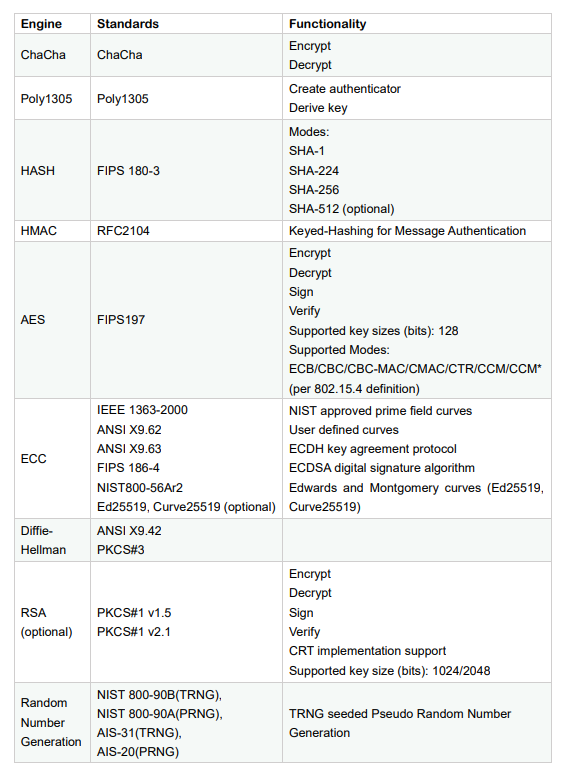
2.5.10 Crypto Engine
Crypto Engine block is an integrated security core and provides a comprehensive security infrastructure that enables system wide protection that includes use cases inside and outside the device.
Function Features are shown as below table.
2.5.11 I2S
I2S is an electrical serial bus interface standard used for connecting digital audio devices together. It is used to communicate PCM audio data between integrated circuits in an electronic device. The I²S bus separates clock and serial data signals.
Operates as an i2s transmitter or receiver
Configurable support for up to 2 stereo channels for both transmitter and receiver
16-bit audio data resolution
Supports full duplex communication due to the independence of transmitter and receiver
Configurable master or slave mode
Supports 8/16/32/40/44.1/48/96 KHz sample rate
2.5.12 PSRAM
The PSRAM interface acts as a synchronous interface to external serial flash or PSRAM device with up to four bidirectional data lines.
Flexible sequence engine to support various flash/PSRAM vendor devices
Single, dual, quad mode of operation.
Memory mapped read access to connected flash devices
Memory mapped read/write access to connected PSRAM devices
Up to 60 MHz clock in SDR mode
Maximum 256 MB device size
3. Wi-Fi Subsystem Descriptions
ASR5822S supports features specified in the IEEE 802.11 base standard, and amended by IEEE 802.11n.
3.1 Wi-Fi MAC
ASR5822S WLAN Media Access Control (MAC) is designed to support high throughput operation with low power consumption.
Transmission and reception of aggregated MPDUs (A-MPDU)
Support for power management schemes, including WMM power-save
Support for immediate ACK and Block-ACK policies
Interframe space timing support, including RIFS
Support for RTS/CTS and CTS-to-self frame sequences for protecting frame exchanges
Back-off counters in hardware for supporting multiple priorities as specified in the WMM specification
Timing synchronization function (TSF), network allocation vector (NAV) maintenance, and target beacon transmission time (TBTT) generation in hardware
Hardware off-load for AES-CCMP, legacy WPA TKIP, legacy WEP ciphers, WAPI, and support for key management
Statistics counters for MIB support
802.11 e: QoS for wireless multimedia technology
Monitor mode: sniff all frames from the medium
3.2 Wi-Fi PHY
ASR5822S WLAN Digital Port Physical Layer (PHY) is designed to comply with IEEE 802.11 b/g/n single stream to provide wireless LAN connectivity or low-power applications.
Supports IEEE 802.11b, 11g, 11n single-stream standards
Supports 802.11n MCS0-7 in both 20 MHz and 40 MHz bandwidth
Supports Optional Greenfield mode in Tx and Rx
Algorithms achieving low power, enhanced sensitivity, range, and reliability
Automatic gain control scheme for blocking and non-blocking application scenario
3.3 Wi-Fi RF
ASR5822S integrates fully 802.11 b/g/n RF transceiver, including T/R switch, matching network, PA, Low Noise Amplifier (LNA) and RF synthesizer. There is no need of off-chip matching network, which saves the BoM and module Print Circuit Board (PCB) size.
The transceiver has auto-calibration and sensor circuits to guarantee the RF performance in mass production. These calibrations include transmit power, IQ imbalance, LO leakage, DC offset, filter bandwidth and etc. The temperature sensor and process sensor are also integrated on-chip.
The following table shows Wi-Fi RF TX and RX specification respectively.
TX Characteristics |
Min. |
Typ. |
Max. |
Unit |
|---|---|---|---|---|
1. Frequency Range |
2412 |
2484 |
MHz |
|
2. Output Power |
||||
1 Mbps CCK |
20 |
dBm |
||
11 Mbps CCK |
20 |
dBm |
||
6 Mbps OFDM |
20 |
dBm |
||
54 Mbps OFDM |
18 |
dBm |
||
HT20, MCS0 |
18 |
dBm |
||
HT20, MCS7 |
17.5 |
dBm |
||
HT40, MCS0 |
18 |
dBm |
||
HT40, MCS7 |
17.5 |
dBm |
||
3. TX EVM |
||||
6 Mbps OFDM |
-7 |
dB |
||
54 Mbps OFDM |
-25 |
dB |
||
HT20, MCS0 |
-7 |
dB |
||
HT20, MCS7 |
-27 |
dB |
||
HT40, MCS0 |
-7 |
dB |
||
HT40, MCS7 |
-27 |
dB |
RX Characteristics |
Min. |
Typ. |
Max. |
Unit |
|---|---|---|---|---|
1. Frequency Range |
2412 |
2484 |
MHz |
|
2. Minimum Input Level Sensitivity |
||||
|
-98 |
dBm |
||
|
-94 |
dBm |
||
|
-89 |
dBm |
||
|
-92.5 |
dBm |
||
|
-76.5 |
dBm |
||
|
-92.5 |
dBm |
||
|
-73 |
dBm |
||
3. Maximum Input Level (FER≤8%) |
||||
6 Mbps OFDM |
10 |
dBm |
||
54 Mbps OFDM |
-8 |
dBm |
||
MCS0 |
10 |
dBm |
||
MCS7 |
-8 |
dBm |
4. Bluetooth Subsystem Descriptions
SoC considers performance improvements for Bluetooth low energy with the Bluetooth 5.1 specifications. Most importantly, it supports:
Supports all packets types (Advertising/Extended Advertising/Data/Control/Long Range)
Supports Constant Tone Extension and IQ sampling. Supports both AOA and AOD CTE type with 1us/2us sampling slots. Supports up to 8 antennae
Supports WLAN Coexistence mechanism
Supports all device classes (Broadcaster, Central, Observer, Peripheral)
Supports Encryption/Decryption (AES-CCM)
Supports bit stream processing (CRC, Whitening)
Supports frequency Hopping calculation (scheme #1 and scheme #2)
Supports FDMA/TDMA/events formatting and synchronization
Supports AHB slave interface for register file access and exchange memory of CPU access via BLE core
Supports power down BLE core during protocol’s idle periods, low power modes support 32.768 KHz low-power clock frequencies.
Supports BLE SIG Mesh: Relay/Proxy/Low power/Friend features
TX Characteristic |
Min. |
Typ. |
Max. |
Unit |
|---|---|---|---|---|
1. Frequency Range |
2402 |
2480 |
MHz |
|
2. Output Power |
0 |
6 |
15 |
dBm |
3. Carrier Frequency Offset and Drift |
||||
|
-150 |
35 |
150 |
KHz |
|
-50 |
1 |
50 |
KHz |
|
-20 |
1 |
20 |
KHz/50us |
4. Modulation Characteristic |
||||
△f1avg |
225 |
249 |
275 |
KHz |
△f2max |
185 |
230 |
KHz |
|
△f1avg/△f2avg |
0.8 |
0.92 |
Hz/Hz |
|
5. In-band Spurious Emission |
||||
±2 MHz Offset |
-39 |
-20 |
dBm |
|
>±3 MHz Offset |
-43 |
-30 |
dBm |
RX Characteristic |
Min. |
Typ. |
Max. |
Unit |
|---|---|---|---|---|
1. Frequency Range |
2402 |
2480 |
MHz |
|
2. Receiver Sensitivity |
-95 |
dBm |
||
3. C/I Co-channel |
4.5 |
21 |
dB |
|
4. C/I 1 MHz |
-10 |
15 |
dB |
|
5. C/I 2 MHz |
-37.5 |
-17 |
dB |
|
6. C/I ≥ 3 MHz |
-41 |
-27 |
dB |
|
7. C/I Image Channel |
-35 |
-9 |
dB |
|
8. C/I Image 1 MHz |
-41 |
-15 |
dB |
|
9. Inter-modulation |
-50 |
-35 |
dBm |
|
10. Out-of-band Blocking |
||||
30 MHz to 2000 MHz |
-30 |
-30 |
dBm |
|
2001 MHz to 2339 MHz |
-35 |
-30 |
dBm |
|
2501 MHz to 3000 MHz |
-35 |
-35 |
dBm |
|
3001 MHz to 12.75 GHz |
-30 |
-30 |
dBm |
5. Electrical Characteristics
5.1 Absolute Maximum Rating
Parameter |
Symbol |
Min. |
Typ. |
Max. |
Unit |
|---|---|---|---|---|---|
Power supply |
VBAT_DCDC |
-0.3 |
5.8 |
V |
|
Storage temperature range |
TSTR |
-55 |
150 |
°C |
|
Operating temperature range (Industrial Grade) |
TOPR |
-40 |
85 |
°C |
5.2 Recommended Operating Conditions
Parameter |
Symbol |
Min. |
Typ. |
Max. |
Unit |
|---|---|---|---|---|---|
Power supply |
VBAT_DCDC |
3 |
3.3/5 |
5.5 |
V |
Operating temperature range (Industrial Grade) |
TOPR |
-40 |
- |
85 |
°C |
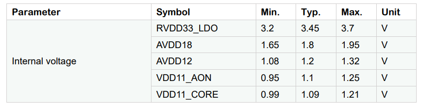
5.3 Supply Voltage Operating Range
5.4 ESD Ratings

5.5 Crystal Specifications
Parameter |
Min. |
Typ. |
Max. |
Unit |
|---|---|---|---|---|
Fundamental frequency |
26 |
MHz |
||
Frequency tolerance |
-10 |
10 |
ppm |
|
Operating temperature |
-30 |
85 |
°C |
|
Load capacitor |
7.5 |
pF |
||
Maximum ESR |
50 |
Ω |
||
Aging per year |
-3 |
3 |
ppm |
5.6 DC Specification
Parameter |
Symbol |
Test Conditions |
Min. |
Max. |
Unit |
|---|---|---|---|---|---|
Input high level, input and I/O pins |
VIH |
Guaranteed logic HIGH level |
2.0 |
DVDD |
V |
Input low level, input and I/O pins |
VIL |
Guaranteed logic LOW level |
VSS |
0.8 |
V |
Output high voltage |
VOH |
VDD=minimum, DVDD=minimum, IOHa=-2mA, -4mA, -8mA, and -12mA |
2.4 |
DVDD |
V |
Output low voltage |
VOL |
VDD=minimum, DVDD=minimum, IOLa=2mA, 4mA, 8mA, and 12mA |
VSS |
0.4 |
V |
High level output current for GPIO |
IOH |
DVDD=3.3 V |
12 |
mA |
|
Low level output current for GPIO |
IOL |
12 |
mA |
||
Input pull-up resistor current |
IRPU |
VPAD=VIH, DVDD=minimum |
50b |
180c |
µA |
Input pull-up resistance |
RPU |
VPAD=VIH, DVDD=minimum |
9d |
19.4e |
KΩ |
Input pull-down resistor current |
IRPD |
VPAD=VIL, DVDD=minimum |
50f |
120c |
µA |
Input pull-down resistance |
RPD |
VPAD=VIL, DVDD=minimum |
6.7d |
16e |
KΩ |
Input hysteresisg |
VH |
0.2g |
V |
||
Input leakage current, non-tolerant |
IPAD |
DVDD=maximum, VPAD=0V or DVDD |
-1h |
1h |
µA |
Fail-safe leakage current |
IPAD |
DVDD=0, VPAD=DVDD maximum |
1i |
µA |
|
Off-State leakage current |
IOZ |
DVDD=maximum, VPAD=0V or DVDD |
1j |
µA |
Valid only when DVDD=2.97V, process=SS, temperature=125°C. This current is de-rated at other PVT conditions, including typical DVDD=1.8V and 2.5V.
Weak pull-up current is the minimum current flowing from DVDD to PAD when DVDD=2.97V, process=SS, and temperature=125°C. This value is de-rated for all the other DVDD values.
Maximum weak pull up and weak pull down currents are the maximum current values from the simulation results with test conditions: DVDD=3.63V, process=FF and temperature=-40°C. It is not a specification.
Minimum value of weak pull up and pull down resistances is the value of minimum resistance from simulation results with test conditions: DVDD=3.63V, process=FF and temperature=-40°C. It is not a specification.
The weak pull-up and pull-down resistance is the maximum resistance with the test conditions specified when DVDD=2.97V, process=SS and temperature=125°C.
Weak pull-down current is the minimum current flowing from PAD to ground, when DVDD=2.97V, process=SS, and temperature=125°C. This value is de-rated for all the other DVDD values.
Valid only when hysteresis is enabled. Simulation conditions for FF: temperature=-40°C and DVDD=3.63V. Simulation condition for SS: temperature=125°C and DVDD=2.97V.
Input leakage current is the current that flows to or out of the PAD node. This leakage is measured when DVDD=3.63V, process=FF and temperature=125°C.
Fail-safe leakage is the current flowing from PAD to DVDD and ground when DVDD is powered down. This leakage is measured with PAD=3.63V, Process=FF, Temperature=125⁰C and DVDD=0.
Input leakage current is the current that flows to or out of the PAD node. This leakage is measured when DVDD=3.63V, process=FF and temperature=125°C.
6. Package Specifications
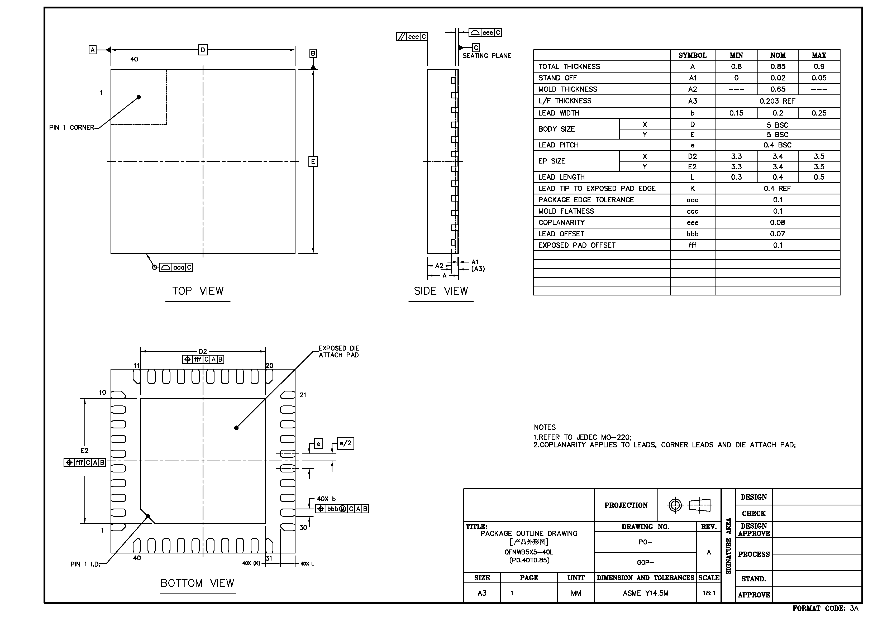
6.1 QFN40 Mechanical Parameters
ASR5822S uses 5 mm x 5 mm QFN package of 40 pins with 0.4 mm pitch.
6.2 QFN40 Pin Assignment and Description
The chip top view and pin descriptions of ASR5822S are shown as follows.
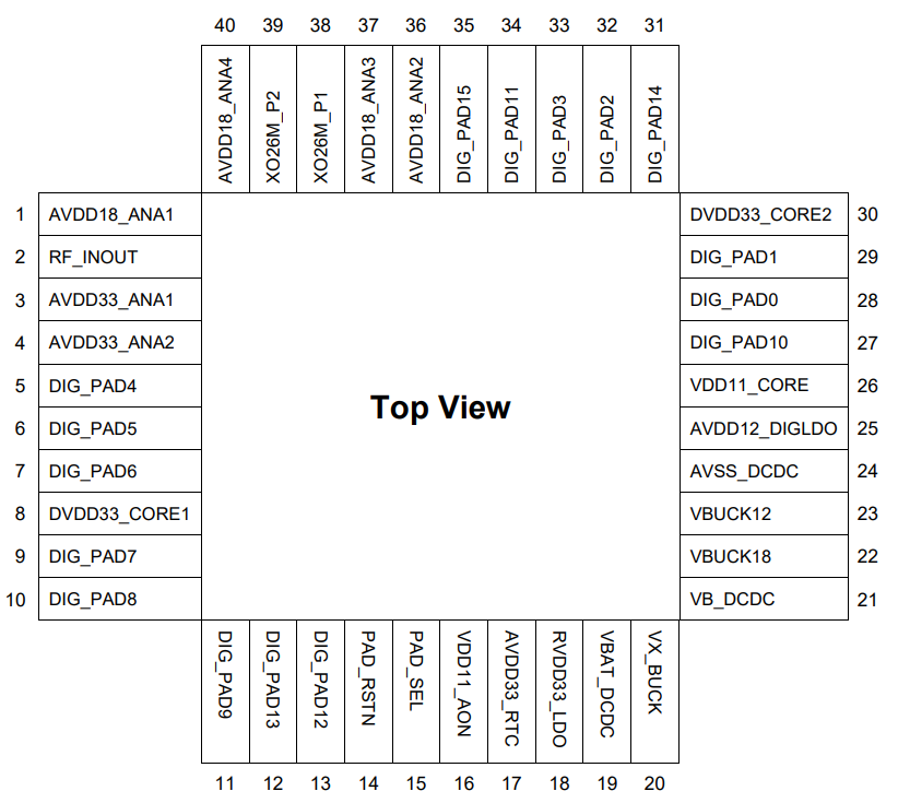
Num. |
Name |
Pin Description |
I/O |
|---|---|---|---|
Power, Clock |
|||
16 |
VDD11_AON |
1.1V digital always-on supply |
Power |
26 |
VDD11_CORE |
1.1V digital core domain supply |
Power |
25 |
AVDD12_DIGLDO |
1.2V digital core LDO supply |
Power |
1 |
AVDD18_ANA1 |
1.8V analog supply |
Power |
36 |
AVDD18_ANA2 |
1.8 V analog supply |
Power |
37 |
AVDD18_ANA3 |
1.8 V analog supply |
Power |
40 |
AVDD18_ANA4 |
1.8 V analog supply |
Power |
3 |
AVDD33_ANA1 |
3.3 V analog supply |
Power |
4 |
AVDD33_ANA2 |
3.3 V analog supply |
Power |
17 |
AVDD33_RTC |
3.3 V RTC domain supply |
Power |
8 |
DVDD33_CORE1 |
3.3 V digital IO supply |
Power |
30 |
DVDD33_CORE2 |
3.3 V digital IO supply |
Power |
38 |
XO26M_P1 |
26 MHz clock output |
Analog |
39 |
XO26M_P2 |
26 MHz clock input |
Analog |
DCDC, LDO |
|||
18 |
RVDD33_LDO |
3.3 V LDO output |
Analog |
19 |
VBAT_DCDC |
3.3~5 V DCDC/LDO supply |
Power |
20 |
VX_BUCK |
DCDC signal |
Analog |
21 |
VB_DCDC |
DCDC signal |
Analog |
22 |
VBUCK18 |
1.8 V DCDC buck output |
Analog |
23 |
VBUCK12 |
1.2 V DCDC buck output |
Analog |
24 |
AVSS_DCDC |
DCDC ground |
Power |
GPIO, Reset, Select |
|||
28 |
DIG_PAD0 |
GPIO |
Digital |
29 |
DIG_PAD1 |
GPIO |
Digital |
32 |
DIG_PAD2 |
GPIO |
Digital |
33 |
DIG_PAD3 |
GPIO |
Digital |
5 |
DIG_PAD4 |
GPIO |
Digital |
6 |
DIG_PAD5 |
GPIO |
Digital |
7 |
DIG_PAD6 |
GPIO |
Digital |
9 |
DIG_PAD7 |
GPIO |
Digital |
10 |
DIG_PAD8 |
GPIO |
Digital |
11 |
DIG_PAD9 |
GPIO |
Digital |
27 |
DIG_PAD10 |
GPIO |
Digital |
34 |
DIG_PAD11 |
GPIO |
Digital |
13 |
DIG_PAD12 |
GPIO |
Digital |
12 |
DIG_PAD13 |
GPIO |
Digital |
31 |
DIG_PAD14 |
GPIO |
Digital |
35 |
DIG_PAD15 |
GPIO |
Digital |
15 |
PAD_SEL |
Mode select |
Digital |
14 |
PAD_RSTN |
Reset |
Digital |
RF Interface |
|||
2 |
RF_INOUT |
Wi-Fi RF input/output |
Analog |