ASR6601 Datasheet
Introduction
About This Document
This document introduces the specifications of LPWAN SoC ASR6601.
Included Chip Models
The product models corresponding to this document are as follows.
Model |
Flash |
SRAM |
Core |
Package |
Frequency |
|---|---|---|---|---|---|
ASR6601SE |
256 KB |
64 KB |
32-bit 48 MHz Arm China STAR-MC1 |
QFN68, 8*8 mm |
150 ~ 960 MHz |
ASR6601CB |
128 KB |
16 KB |
32-bit 48 MHz Arm China STAR-MC1 |
QFN48, 6*6 mm |
150 ~ 960 MHz |
ASR6601SER |
256 KB |
64 KB |
32-bit 48 MHz Arm China STAR-MC1 |
QFN68, 8*8 mm |
150 ~ 960 MHz |
ASR6601CBR |
128 KB |
16 KB |
32-bit 48 MHz Arm China STAR-MC1 |
QFN48, 6*6 mm |
150 ~ 960 MHz |
Copyright Notice
© 2023 ASR Microelectronics Co., Ltd. All rights reserved. No part of this document can be reproduced, transmitted, transcribed, stored, or translated into any language in any form or by any means without the written permission of ASR Microelectronics Co., Ltd.
Trademark Statement
ASR and ASR Microelectronics Co., Ltd. are trademarks of ASR Microelectronics Co., Ltd.
Other trade names, trademarks, and registered trademarks mentioned in this document are the property of their respective owners and are hereby declared.
Disclaimer
ASR does not give any warranty of any kind and may make improvements and/or changes in this document or in the product described in this document at any time.
This document is only used as a guide, and no contents in the document constitute any form of warranty. Information in this document is subject to change without notice.
All liability, including liability for infringement of any proprietary rights caused by using the information in this document, is disclaimed.
Revision History
Date |
Version |
Release Notes |
|---|---|---|
2023.09 |
V1.7.0 |
Added chip models of ASR6601SER and ASR6601CBR and Section 3.6: RSTN Characteristics. |
1. Overview
1.1 General
ASR6601 is a general LPWAN Wireless Communication SoC, with integrated RF Transceiver, Modem and a 32-bit RISC MCU. The MCU uses ARM China STAR-MC1, with 48 MHz operation frequency. The RF Transceiver has continuous frequency coverage from 150 MHz to 960 MHz. The Modem supports LoRa modulation for LPWAN use cases and (G)FSK modulation for legacy use cases. The Modem also supports BPSK modulation in TX and (G)MSK modulation in TX and RX. The LPWAN Wireless Communication Module designed with ASR6601 provides ultra-long range and ultra-low power communication for LPWAN application.
ASR6601 can achieve a high sensitivity to -148 dBm and the maximum transmit power is up to +22 dBm. This makes the chip suitable to be used in long range LPWAN and have high efficiency. The total chip package is of very small size, QFN 6 mm x 6 mm/QFN 8 mm x 8 mm.
1.2 Key Features
Small footprint: QFN48, 6 mm x 6 mm or QFN68, 8 mm x 8 mm
Frequency Range: 150 MHz ~ 960 MHz
Maximum Power +22 dBm constant RF output
High sensitivity: -148 dBm
Programmable bit rate up to 62.5 Kbps in LoRa modulation mode
Programmable bit rate up to 300 Kbps in (G)FSK modulation mode
Preamble detection
Embedded memories (up to 256 KB of Flash memory and 64 KB of SRAM).
Up to 42 configurable GPIOs: 3 x I2C, 1 x I2S, 4 x UART, 1 x LPUART, 1 x SWD, 3 x SPI, 1 x QSPI and 2 x WDG
4 x GPtimer, 2 x Basic Timer, 2 x LP timer and 1 x Sys Ticker
48 MHz Arm China STAR-MC1 CPU
4-channel DMA engine x 2
Embedded 12-bit 1 Msps SAR ADC
Embedded 12-bit DAC
32.768 KHz External Watch Crystal Oscillator
32 MHz External Crystal Oscillator for RF Transceiver
24 MHz External Crystal Oscillator for SoC (optional)
Embedded internal 4 MHz RC oscillator
Embedded internal High frequency (48 MHz) RC oscillator
Embedded internal Low frequency (32.768 KHz) RC oscillator
Embedded internal PLL to generate 48 MHz clock
Embedded 3 x OPA
Embedded 2 x Low Power Comparator
Embedded LCD driver
Embedded LD, TD, VD and FD
Supports AES, DES, RSA, ECC, SHA and SM2/3/4
1.3 Block Diagram
The following figure shows the block diagram of ASR6601 SoC and ASR6601 LPWAN Module.

1.4 Specification
The table below shows the general specifications of ASR6601 SoC.
Item |
Description |
|---|---|
Temperature |
Storage: -55 ~ +125℃; Operating: -40 ~ +85℃ |
Humidity |
Storage: 5 ~ 95% (Non-Condensing); Operating: 10 ~ 95% (Non-Condensing) |
Dimension |
8x8x0.9 mm / 6x6x0.9 mm |
Package |
QFN 68 Pin Type/QFN 48 Pin Type |
1.5 Applications
ASR6601 LPWAN chip enables new generation of IoT applications.
Smart meters
Supply chain and logistics
Building automation
Agricultural sensors
Smart cities
Retail store sensors
Asset tracking
Streetlights
Parking sensors
Environmental sensors
Healthcare
Smoke sensors
Safety and security sensors
Remote control applications
1.6 Part Number Information
There are four part numbers of ASR6601: ASR6601CB, ASR6601CBR, ASR6601SE, and ASR6601SER. The key feature differences between two parts numberamong the four part numbers of ASR6601 are listlisted below,. ASR6601SE and ASR6601SER can support more analog functions with more GPIOs.

Note
Compared to the ASR6601SE (ASR6601CB), the new part number ASR6601SER (ASR6601CBR) changes only in the RSTN pin function; the RSTN pin number remains the same. All other pins are the same as those of previous part numbers.
For the ASR6601SER (ASR6601CBR), the reset signal on the RSTN pin only resets main domain, and the Aon domain and Aonr domain keeps running. For the ASR6601SE (ASR6601CB), the reset signal on the RSTN pin will restart the whole chip, with the same function as power-on reset. As for the definition of the main domain, the Aon domain and the Aonr domain, please refer to Section 4.2: Power Supply Architecture in ASR6601 Reference Manual.
For the software reference design, the ASR6601SER (ASR6601CBR) can only be supported by the SDK v2.0.0 or the later versions. For more details, please refer to the SDK release note.
2. System Description
2.1 Power Supply
ASR6601 has several separated power supply pins. With these separated power supply pins, the interference from digital parts of SoC to RF blocks is reduced.
ASRR6601 Power Grid is shown in the figure below:

VDD_IN: The power supply for the PA in the RF transmitter.
VBAT_RF: The power supply for the RF TRX, excluding the PA.
VDCC_RF: The low power supply for RF TRX, which must be connected to VREG pin of SoC through the PCB.
VBAT_ESD0: Power supply for digital IO.
VBAT_ESD1: Power supply for digital IO.
VBAT_ESD2: Power supply for digital IO.
VBAT_ESD3: Power supply for digital IO.
VBAT_DCC: The power supply for DCDC.
VBAT_ESD_RTC: The power supply for IOs in RTC domain.
VBAT_RTC: The power supply for analog blocks in RTC domain.
VBAT_ANA: The power supply for analog blocks.
2.2 Boot Mode
The boot mode can be configured by the levels of BOOT0 pin and the data in the Flash.
DebugLevel |
UseFlashBoot0 |
FlashBoot0 |
BOOT0 pin |
FlashBoot1 |
MainFlashEmpty |
Boot Config |
|---|---|---|---|---|---|---|
2 |
X |
X |
X |
X |
X |
boot from Flash Main |
<2 |
0 |
X |
0 |
X |
0 |
boot from Flash Main |
<2 |
0 |
X |
0 |
X |
1 |
boot from Bootloader |
<2 |
0 |
X |
1 |
1 |
X |
boot from Bootloader |
<2 |
0 |
X |
1 |
0 |
X |
boot from Sys SRAM |
<2 |
1 |
1 |
X |
X |
0 |
boot from Flash Main |
<2 |
1 |
1 |
X |
X |
1 |
boot from Bootloader |
<2 |
1 |
0 |
X |
1 |
X |
boot from Bootloader |
<2 |
1 |
0 |
X |
0 |
X |
boot from Sys SRAM |
DebugLevel, UseFlashBoot0, FlashBoot0 and FlashBoot1 is the information area of the Flash, they can be modified according to the application. MainFlashEmpty is determined by the data of address 0 in the flash Main area. If the data in the address 0 of Flash Main area is 0xFFFFFFFF, the value of MainFlashEmpty is 1, otherwise the value of MainFlashEmpty is 0. BOOT0 pin is GPIO02 in the package.
The boot mode is selected according to the configurations when the system is in these status: first powered up, exit the Standby mode or reset.
3. Electrical Characteristics
Electrical Characteristics include absolute maximum rating, recommended operating range, TRX performance, power consumption characteristics, ESD ratings and RSTN characteristics for the SoC and module.
3.1 Absolute Maximum Rating
Parameter |
Symbol |
Min. |
Typ. |
Max. |
Unit |
|---|---|---|---|---|---|
Supply Voltage |
VDD |
-0.3 |
3.9 |
V |
|
Digital Input Voltage Level |
Vin |
-0.3 |
3.9 |
V |
|
RF Input Power |
Pin |
+10 |
dBm |
3.2 Recommended Operating Range
Parameter |
Symbol |
Min. |
Typ. |
Max. |
Unit |
|---|---|---|---|---|---|
Supply Voltage |
VDD |
1.7 |
3.3 |
3.7 |
V |
RF Input Power |
Pin |
+10 |
dBm |
3.3 TRX Performance

3.4 Power Consumption Characteristics

Note
IDD_Standby and IDD_Stop3 are tested at 25 degrees and the RCO32K is used as the RTC clk.
The XO32K block operates either in its normal mode or low-power mode. Through the proper design of XO32K PCB routing, the XO32K can work in its low-power mode, and in this case, the IDD current with the XO32K clk is as low as that with the RCO32K clk. For more details, please refer to ASR6601 Hardware Design Guide. Otherwise, the XO32K block shall only work in the normal mode, and the current will increase about 500nA compared with the low-power mode.
SoC Core Supply Current refers to the power consumption of the Arm China STAR-MC1 processor and SoC TRX Supply Current refers to the power consumption of the LPWAN RF Transceiver.
3.5 ESD Ratings
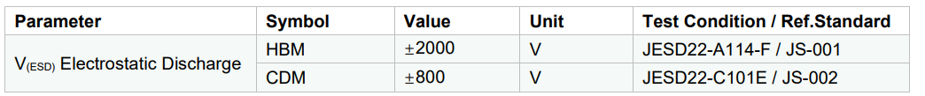
3.6 RSTN Characteristics
For ASR6601CB/ASR6601SE RSTN, the reset signal on RSTN pin restarts the whole chip including the main domain, the Aon domain and the Aonr domain, with the function as power-on reset. With a slow rise or fall of the signal on the NRST pin when the VBAT is ready, a particular unwanted internal reset timing is generated, which will make the chip enter safe mode and erase the flash. The reference design of NRST is as below,
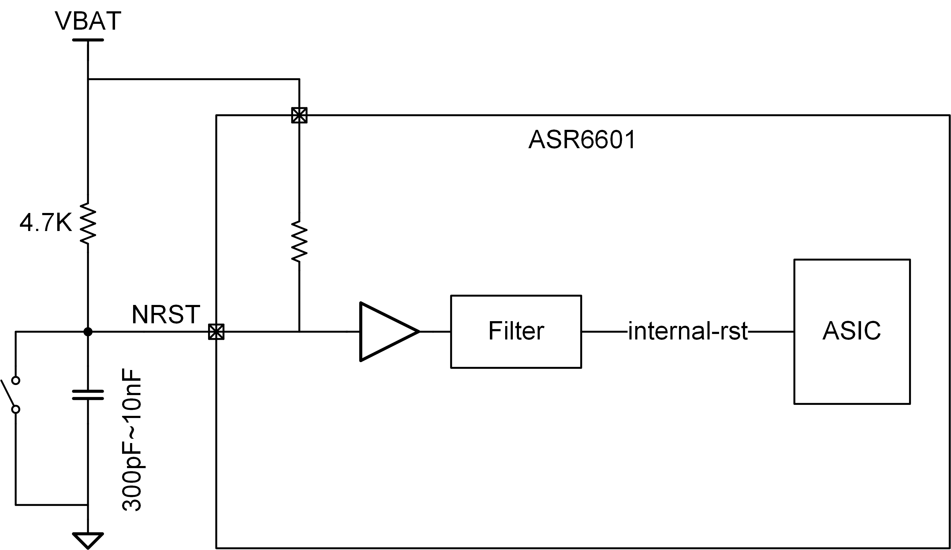
Note
The parallel resistance value is recommended to be 4.7K~10K, and the parallel capacitance value is recommended to be 300pF~10nF.
Different VDD power-on timings and unwanted reset timing must be avoided, or risks will arise. For more details, please refer to ASR6601 Hardware Design Guide.
For ASR6601CBR/ASR6601SER RSTN, the reset signal on RSTN pin only resets the main domain, which is different from the ASR6601CB/ASR6601SE RSTN. The RSTN is controlled by an external switch or one GPIO from other MCU, which can be configured to open drain output mode or push pull output mode. The reference design of RSTN pin is as below:
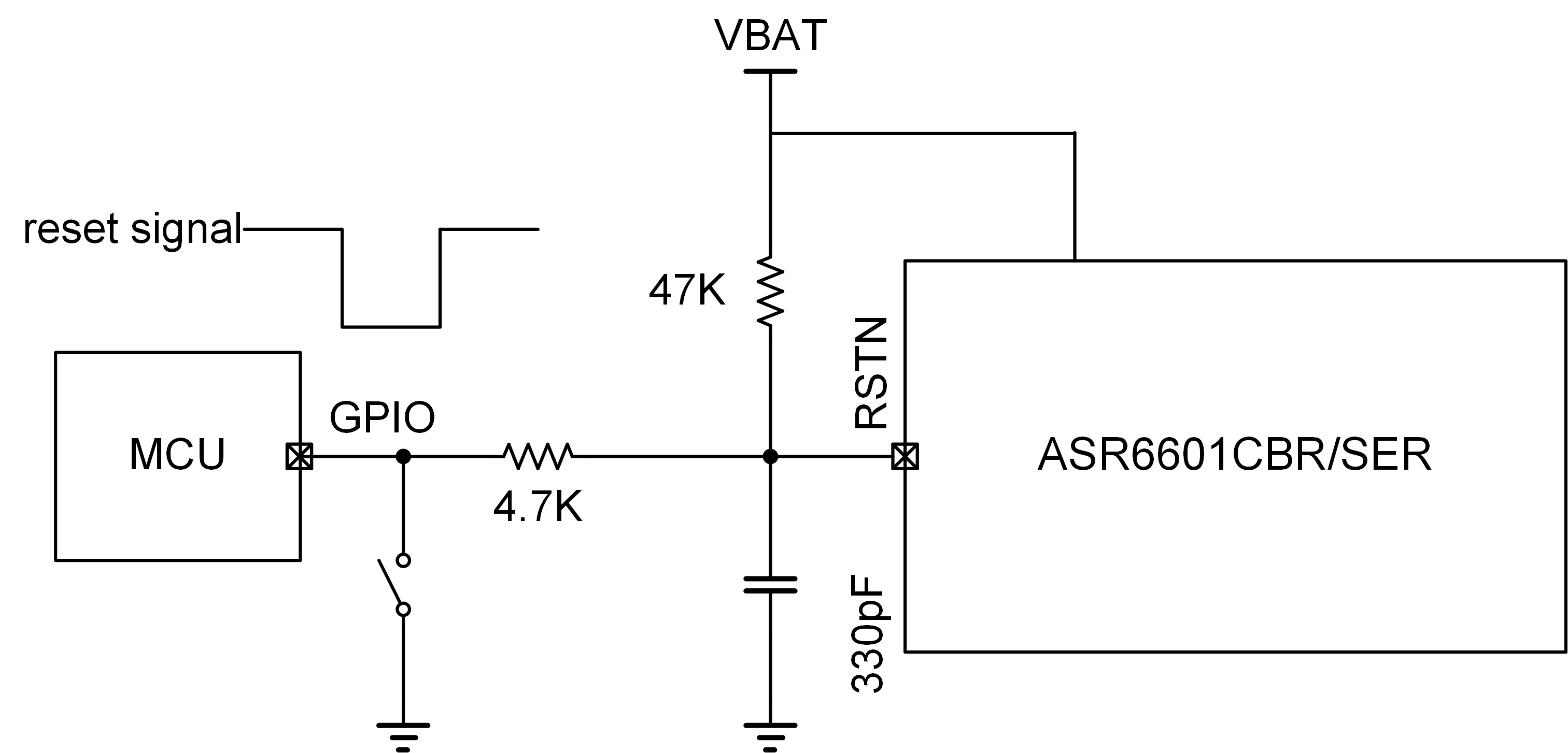
Note
If MCU GPIO is configured to open drain output mode, the serial resistor may not be used, but the pull-up resistor is a must, otherwise the high RSTN will be HIZ.
ASR6601SER (ASR6601CBR) can only be supported by the SDK v2.0.0 or the later versions. For more details, please refer to the SDK release note.
4. Package and Pin Definition
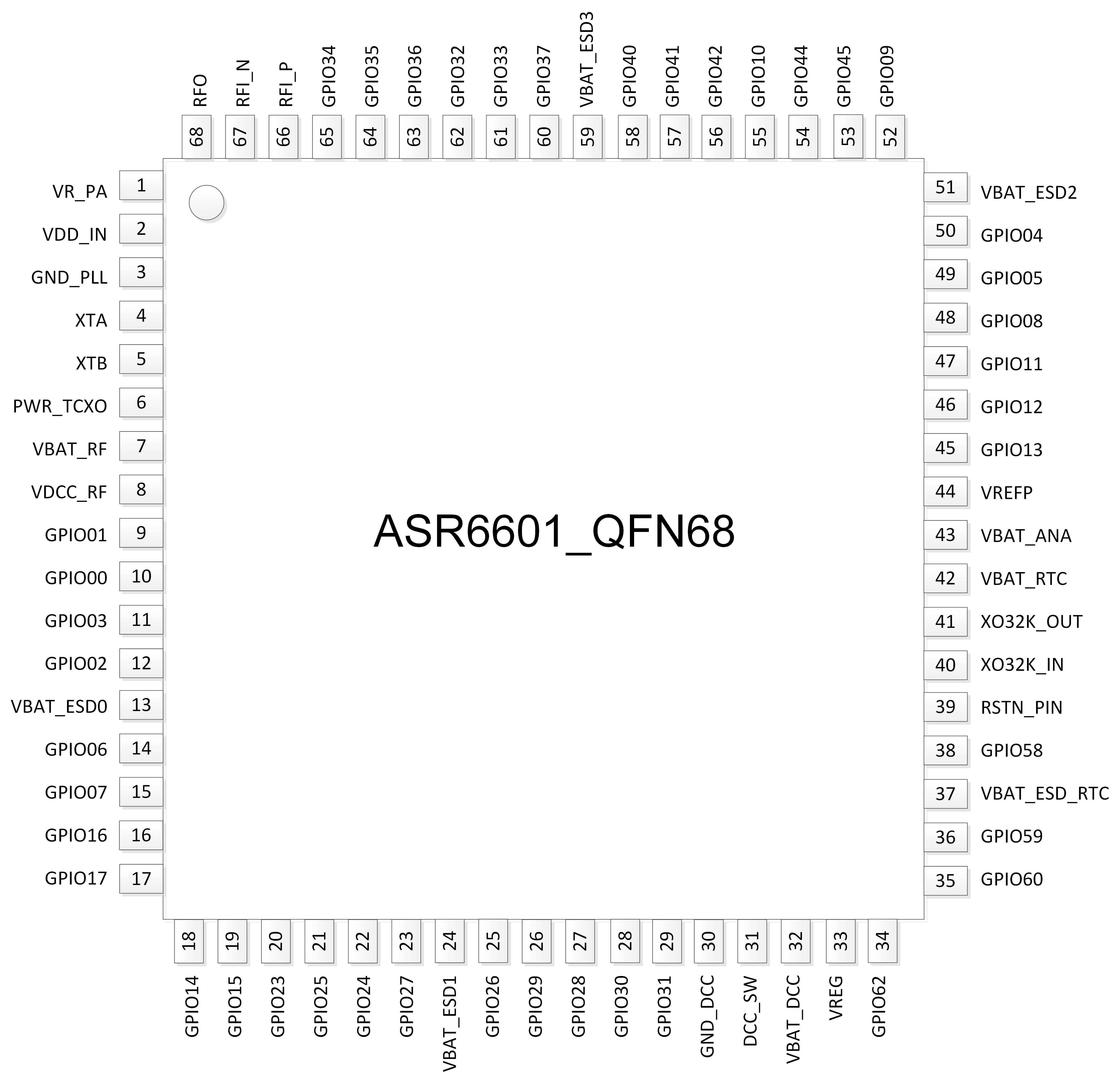
4.1 ASR6601SE QFN68
Below are two models of the ASR6601 in QFN68 package, which share the same pin definition, pin assignment and mechanical parameters.
Model |
Flash |
SRAM |
Processor |
Package |
Frequency |
|---|---|---|---|---|---|
ASR6601SE |
256 KB |
64 KB |
32-bit 48 MHz Arm China STAR-MC1 |
QFN68, 8*8 mm |
150 ~ 960 MHz |
ASR6601SER |
256 KB |
64 KB |
32-bit 48 MHz Arm China STAR-MC1 |
QFN68, 8*8 mm |
150 ~ 960 MHz |
4.1.1 ASR6601 QFN68 Pin Definition
Pin No. |
Pin Name |
Pin Type |
Description |
Power Domain (V) |
|---|---|---|---|---|
1 |
VR_PA |
IO |
Regulated power amplifier supply |
3.3 |
2 |
VDD_IN |
Power |
Input voltage for power amplifier, VR_PA |
3.3 |
3 |
GND_PLL |
Ground |
Ground for PLL |
3.3 |
4 |
XTA |
IO_IN |
XO32M for RF input |
1.8 |
5 |
XTB |
IO_IN |
XO32M for RF input |
1.8 |
6 |
PWR_TCXO |
IO_OUT |
Output power for TCXO supply |
1.8 |
7 |
VBAT_RF |
Power |
Supply for RF |
3.3 |
8 |
VDCC_RF |
Power |
DCDC input for RF |
1.55 |
9 |
GPIO01 |
IO |
General-purpose input/output |
3.3 |
10 |
GPIO00 |
IO |
General-purpose input/output |
3.3 |
11 |
GPIO03 |
IO |
General-purpose input/output |
3.3 |
12 |
GPIO02 |
IO |
General-purpose input/output |
3.3 |
13 |
VBAT_ESD0 |
Power |
Power supply for IO |
3.3 |
14 |
GPIO06 |
IO |
SWD_DATA |
3.3 |
15 |
GPIO07 |
IO |
SWD_CLK |
3.3 |
16 |
GPIO16 |
IO |
General-purpose input/output |
3.3 |
17 |
GPIO17 |
IO |
General-purpose input/output |
3.3 |
18 |
GPIO14 |
IO |
General-purpose input/output |
3.3 |
19 |
GPIO15 |
IO |
General-purpose input/output |
3.3 |
20 |
GPIO23 |
IO |
General-purpose input/output |
3.3 |
21 |
GPIO25 |
IO |
General-purpose input/output |
3.3 |
22 |
GPIO24 |
IO |
General-purpose input/output |
3.3 |
23 |
GPIO27 |
IO |
General-purpose input/output |
3.3 |
24 |
VBAT_ESD1 |
Power |
Power supply for IO |
3.3 |
25 |
GPIO26 |
IO |
General-purpose input/output |
3.3 |
26 |
GPIO29 |
IO |
General-purpose input/output |
3.3 |
27 |
GPIO28 |
IO |
General-purpose input/output |
3.3 |
28 |
GPIO30 |
IO |
General-purpose input/output |
3.3 |
29 |
GPIO31 |
IO |
General-purpose input/output |
3.3 |
30 |
GND_DCC |
Ground |
DCC ground |
3.3 |
31 |
DCC_SW |
Power |
DCC Switcher Output |
1.55 |
32 |
VBAT_DCC |
Power |
Supply for DCC |
3.3 |
33 |
VREG |
Power |
Regulated output voltage from the internal LDO/DCC |
1.55 |
34 |
GPIO62 |
IO |
General-purpose input/output |
3.3 |
35 |
GPIO60 |
IO |
General-purpose input/output |
3.3 |
36 |
GPIO59 |
IO |
General-purpose input/output |
3.3 |
37 |
VBAT_ESD_RTC |
Power |
Power supply for IO |
3.3 |
38 |
GPIO58 |
IO |
General-purpose input/output |
3.3 |
39 |
RSTN_PIN |
IO_IN |
External reset pin |
3.3 |
40 |
XO32K_IN |
IO_IN |
XO32K for MCU input |
1.2 |
41 |
XO32K_OUT |
IO_IN |
XO32K for MCU input |
1.2 |
42 |
VBAT_RTC |
Power |
Power supply for Analog |
3.3 |
43 |
VBAT_ANA |
Power |
Power supply for Analog |
3.3 |
44 |
VREFP |
IO_IN |
Power supply for IO |
3.3 |
45 |
GPIO13 |
IO |
General-purpose input/output |
3.3 |
46 |
GPIO12 |
IO |
General-purpose input/output |
3.3 |
47 |
GPIO11 |
IO |
General-purpose input/output |
3.3 |
48 |
GPIO08 |
IO |
General-purpose input/output |
3.3 |
49 |
GPIO05 |
IO |
General-purpose input/output |
3.3 |
50 |
GPIO04 |
IO |
General-purpose input/output |
3.3 |
51 |
VBAT_ESD2 |
Power |
Power supply for IO |
3.3 |
52 |
GPIO09 |
IO |
General-purpose input/output |
3.3 |
53 |
GPIO45 |
IO |
General-purpose input/output |
3.3 |
54 |
GPIO44 |
IO |
General-purpose input/output |
3.3 |
55 |
GPIO10 |
IO |
General-purpose input/output |
3.3 |
56 |
GPIO42 |
IO |
General-purpose input/output |
3.3 |
57 |
GPIO41 |
IO |
General-purpose input/output |
3.3 |
58 |
GPIO40 |
IO |
General-purpose input/output |
3.3 |
59 |
VBAT_ESD3 |
Power |
Power supply for IO |
3.3 |
60 |
GPIO37 |
IO |
General-purpose input/output |
3.3 |
61 |
GPIO33 |
IO |
General-purpose input/output |
3.3 |
62 |
GPIO32 |
IO |
General-purpose input/output |
3.3 |
63 |
GPIO36 |
IO |
General-purpose input/output |
3.3 |
64 |
GPIO35 |
IO |
General-purpose input/output |
3.3 |
65 |
GPIO34 |
IO |
General-purpose input/output |
3.3 |
66 |
RFI_P |
IO |
RF receiver input |
3.3 |
67 |
RFI_N |
IO |
RF receiver input |
3.3 |
68 |
RFO |
IO |
RF transmitter output |
3.3 |
4.1.2 ASR6601 QFN68 Pin Assignment
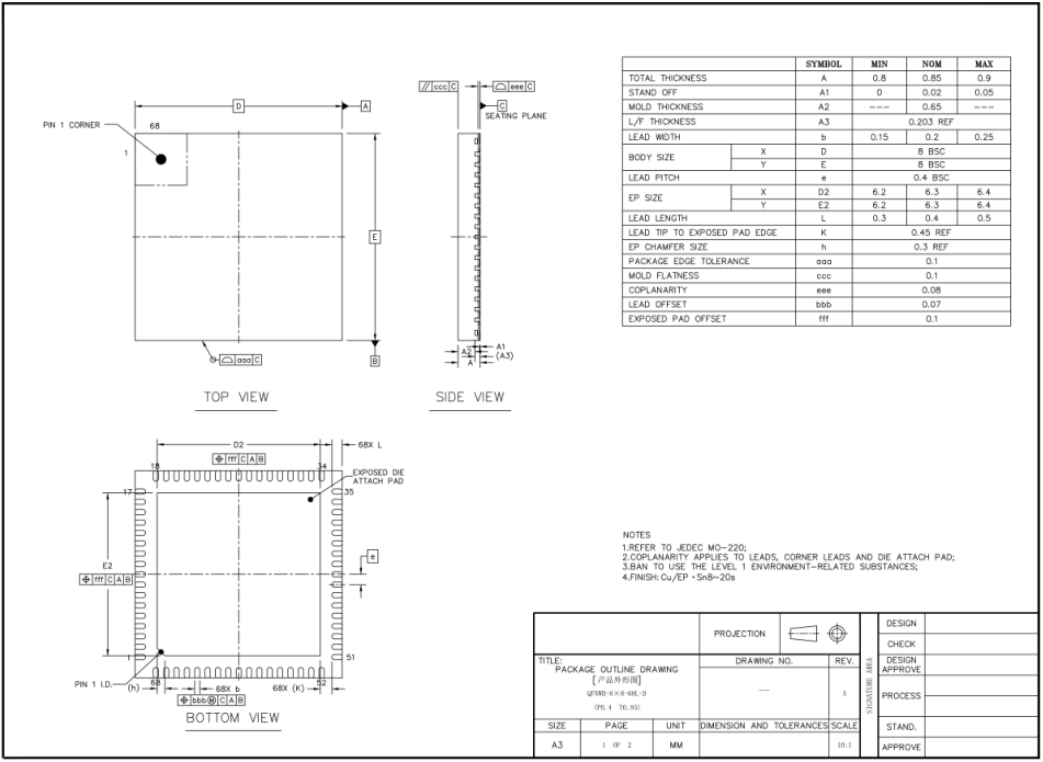
4.1.3 ASR6601 QFN68 Mechanical Parameters
4.2 ASR6601 QFN48
Below are two models of the ASR6601 in QFN48 package, which share the same pin definition, pin assignment and mechanical parameters.
Model |
Flash |
SRAM |
Processor |
Package |
Frequency |
|---|---|---|---|---|---|
ASR6601CB |
128 KB |
16 KB |
32-bit 48 MHz Arm China STAR-MC1 |
QFN48, 6*6 mm |
150 ~ 960 MHz |
ASR6601CBR |
128 KB |
16 KB |
32-bit 48 MHz Arm China STAR-MC1 |
QFN48, 6*6 mm |
150 ~ 960 MHz |
4.2.1 ASR6601 QFN48 Pin Definition
Pin No. |
Pin Name |
Pin Type |
Description |
Power Domain (V) |
|---|---|---|---|---|
1 |
VR_PA |
IO |
Regulated power amplifier supply |
3.3 |
2 |
VDD_IN |
Power |
Input voltage for power amplifier, VR_PA |
3.3 |
3 |
GND_PLL |
Ground |
Ground for PLL |
3.3 |
4 |
XTA |
IO_IN |
XO32M for RF input |
1.8 |
5 |
XTB |
IO_IN |
XO32M for RF input |
1.8 |
6 |
PWR_TCXO |
IO_OUT |
Output power for TCXO supply |
1.8 |
7 |
VBAT_RF |
Power |
Supply for RF |
3.3 |
8 |
VDCC_RF |
Power |
DCC input for RF |
1.55 |
9 |
GPIO01 |
IO |
General-purpose input/output |
3.3 |
10 |
GPIO00 |
IO |
General-purpose input/output |
3.3 |
11 |
GPIO03 |
IO |
General-purpose input/output |
3.3 |
12 |
GPIO02 |
IO |
General-purpose input/output |
3.3 |
13 |
GPIO06 |
IO |
SWD_DATA |
3.3 |
14 |
GPIO07 |
IO |
SWD_CLK |
3.3 |
15 |
VBAT_ESD0 |
Power |
Power supply for IO |
3.3 |
16 |
GPIO16 |
IO |
General-purpose input/output |
3.3 |
17 |
GPIO17 |
IO |
General-purpose input/output |
3.3 |
18 |
GPIO14 |
IO |
General-purpose input/output |
3.3 |
19 |
GPIO15 |
IO |
General-purpose input/output |
3.3 |
20 |
GND_DCC |
Ground |
DCC ground |
3.3 |
21 |
DCC_SW |
Power |
DCC Switcher Output |
1.55 |
22 |
VBAT_DCC |
Power |
Supply for DCC |
3.3 |
23 |
VREG |
Power |
Regulated output voltage from the internal LDO/DCC |
1.55 |
24 |
GPIO62 |
IO |
General-purpose input/output |
3.3 |
25 |
GPIO60 |
IO |
General-purpose input/output |
3.3 |
26 |
GPIO59 |
IO |
General-purpose input/output |
3.3 |
27 |
GPIO58 |
IO |
General-purpose input/output |
3.3 |
28 |
RSTN_PIN |
IO_IN |
External reset pin |
3.3 |
29 |
XO32K_IN |
IO_IN |
XO32K for MCU input |
1.2 |
30 |
XO32K_OUT |
IO_IN |
XO32K for MCU input |
1.2 |
31 |
VBAT_RTC |
Power |
Power supply for Analog |
3.3 |
32 |
VBAT_ANA |
Power |
Power supply for Analog |
3.3 |
33 |
GPIO11 |
IO |
General-purpose input/output |
3.3 |
34 |
GPIO08 |
IO |
General-purpose input/output |
3.3 |
35 |
GPIO05 |
IO |
General-purpose input/output |
3.3 |
36 |
GPIO04 |
IO |
General-purpose input/output |
3.3 |
37 |
GPIO09 |
IO |
General-purpose input/output |
3.3 |
38 |
GPIO47 |
IO |
General-purpose input/output |
3.3 |
39 |
VBAT_ESD3 |
Power |
Power supply for IO |
3.3 |
40 |
GPIO45 |
IO |
General-purpose input/output |
3.3 |
41 |
GPIO44 |
IO |
General-purpose input/output |
3.3 |
42 |
GPIO10 |
IO |
General-purpose input/output |
3.3 |
43 |
GPIO37 |
IO |
General-purpose input/output |
3.3 |
44 |
GPIO33 |
IO |
General-purpose input/output |
3.3 |
45 |
GPIO32 |
IO |
General-purpose input/output |
3.3 |
46 |
RFI_P |
IO |
RF receiver input |
3.3 |
47 |
RFI_N |
IO |
RF receiver input |
3.3 |
48 |
RFO |
IO |
RF transmitter output |
3.3 |
4.2.2 ASR6601 QFN48 Pin Assignment

4.2.3 ASR6601 QFN48 Mechanical Parameters

4.3 GPIO Function MUX Table
GPIO No. |
Fun=0 |
Fun=1 |
Fun=2 |
Fun=3 |
|---|---|---|---|---|
GPIO00 |
GPIO_PORTA_0 |
UART0_RXD |
UART0_TXD |
UART0_SIR_OUT |
GPIO01 |
GPIO_PORTA_1 |
UART0_TXD |
UART0_RXD |
UART0_SIR_IN |
GPIO02 |
GPIO_PORTA_2 |
UART0_CTS |
I2S_DI |
I2C0_SCL |
GPIO03 |
GPIO_PORTA_3 |
UART0_RTS |
I2S_DO |
I2C0_SDA |
GPIO04 |
GPIO_PORTA_4 |
UART1_RXD |
UART1_TXD |
UART1_SIR_OUT |
GPIO05 |
GPIO_PORTA_5 |
UART1_TXD |
UART1_RXD |
UART1_SIR_IN |
GPIO06 |
GPIO_PORTA_6 |
UART1_CTS |
SWD |
I2C1_SCL |
GPIO07 |
GPIO_PORTA_7 |
UART1_RTS |
SWC |
I2C1_SDA |
GPIO08 |
GPIO_PORTA_8 |
UART2_RXD |
UART2_TXD |
UART2_SIR_OUT |
GPIO09 |
GPIO_PORTA_9 |
UART2_TXD |
UART2_RXD |
UART2_SIR_IN |
GPIO10 |
GPIO_PORTA_10 |
UART2_CTS |
I2C2_SCL |
|
GPIO11 |
GPIO_PORTA_11 |
UART2_RTS |
I2C2_SDA |
|
GPIO12 |
GPIO_PORTA_12 |
UART3_RXD |
UART3_TXD |
UART3_SIR_OUT |
GPIO13 |
GPIO_PORTA_13 |
UART3_TXD |
UART3_RXD |
UART3_SIR_IN |
GPIO14 |
GPIO_PORTA_14 |
UART3_CTS |
I2C0_SCL |
|
GPIO15 |
GPIO_PORTA_15 |
UART3_RTS |
I2C0_SDA |
|
GPIO16 |
GPIO_PORTB_0 |
UART0_RXD |
UART0_TXD |
UART0_SIR_OUT |
GPIO17 |
GPIO_PORTB_1 |
UART0_TXD |
UART0_RXD |
UART0_SIR_IN |
GPIO23 |
GPIO_PORTB_7 |
UART1_RTS |
I2C2_SDA |
|
GPIO24 |
GPIO_PORTB_8 |
UART2_RXD |
UART2_TXD |
UART2_SIR_OUT |
GPIO25 |
GPIO_PORTB_9 |
UART2_TXD |
UART2_RXD |
UART2_SIR_IN |
GPIO26 |
GPIO_PORTB_10 |
UART2_CTS |
LPTIM1_IN2 |
I2C0_SCL |
GPIO27 |
GPIO_PORTB_11 |
UART2_RTS |
LPTIM1_OUT |
I2C0_SDA |
GPIO28 |
GPIO_PORTB_12 |
UART3_RXD |
UART3_TXD |
UART3_SIR_OUT |
GPIO29 |
GPIO_PORTB_13 |
UART3_TXD |
UART3_RXD |
UART3_SIR_IN |
GPIO30 |
GPIO_PORTB_14 |
UART3_CTS |
QSPI_IO1 |
I2C1_SCL |
GPIO31 |
GPIO_PORTB_15 |
UART3_RTS |
QSPI_IO2 |
I2C1_SDA |
GPIO32 |
GPIO_PORTC_0 |
UART0_RXD |
UART0_TXD |
UART0_SIR_OUT |
GPIO33 |
GPIO_PORTC_1 |
UART0_TXD |
UART0_RXD |
UART0_SIR_IN |
GPIO34 |
GPIO_PORTC_2 |
UART0_CTS |
I2C2_SCL |
|
GPIO35 |
GPIO_PORTC_3 |
UART0_RTS |
I2C2_SDA |
|
GPIO36 |
GPIO_PORTC_4 |
UART1_RXD |
UART1_TXD |
UART1_SIR_OUT |
GPIO37 |
GPIO_PORTC_5 |
UART1_TXD |
UART1_RXD |
UART1_SIR_IN |
GPIO40 |
GPIO_PORTC_8 |
UART2_RXD |
UART2_TXD |
UART2_SIR_OUT |
GPIO41 |
GPIO_PORTC_9 |
UART2_TXD |
UART2_RXD |
UART2_SIR_IN |
GPIO42 |
GPIO_PORTC_10 |
UART2_CTS |
I2C1_SCL |
|
GPIO44 |
GPIO_PORTC_12 |
UART3_RXD |
UART3_TXD |
UART3_SIR_OUT |
GPIO45 |
GPIO_PORTC_13 |
UART3_TXD |
UART3_RXD |
UART3_SIR_IN |
GPIO47 |
GPIO_PORTC_15 |
UART3_RTS |
LPUART_TX |
I2C2_SDA |
GPIO58 |
GPIO_PORTD_10 |
RTC_TAMPER |
LPTIM_IN1 |
RTC_IO_OUT |
GPIO59 |
GPIO_PORTD_11 |
RTC_WAKEUP0 |
LPTIM_ETR |
LORA_RF_SWITCH |
GPIO60 |
GPIO_PORTD_12 |
RTC_WAKEUP1 |
LPUART_RX |
LORA_RF_SWITCH |
GPIO62 |
GPIO_PORTD_14 |
LPTIM_IN2 |
LPUART_RX |
LPTIM_ETR |
GPIO No. |
Fun=4 |
Fun=5 |
Fun=6 |
Fun=7 |
Analog |
|---|---|---|---|---|---|
GPIO00 |
SSP0_CLK |
GPTIM0_CH0 |
GPTIM0_ETR |
||
GPIO01 |
SSP0_NSS |
I2S_MCLK |
GPTIM0_CH1 |
GPTIM2_ETR |
|
GPIO02 |
SSP0_TX |
GPTIM0_CH2 |
GPTIM2_CH0 |
||
GPIO03 |
SSP0_RX |
GPTIM0_CH3 |
GPTIM2_CH1 |
||
GPIO04 |
SSP1_CLK |
I2S_WS_IN |
I2S_WS_OUT |
GPTIM3_ETR |
COM4/SEG23/ADC_IN3 |
GPIO05 |
SSP1_NSS |
MCO |
GPTIM0_CH0 |
GPTIM0_ETR |
COMP0_INN/COM5/SEG22/ADC_IN2 |
GPIO06 |
SSP1_TX |
I2S_SCLK_IN |
I2S_SCLK_OUT |
||
GPIO07 |
SSP1_RX |
LPTIM_OUT |
|||
GPIO08 |
SSP2_CLK |
GPTIM1_CH0 |
GPTIM3_CH0 |
COMP0_INP/SEG6/ADC_IN1 |
|
GPIO09 |
SSP2_NSS |
COMP1_OUT |
GPTIM1_CH1 |
GPTIM3_CH1 |
SEG14/DAC_OUT |
GPIO10 |
SSP2_TX |
GPTIM0_CH0 |
GPTIM0_ETR |
COM3/SEG24/OPA0_OUT |
|
GPIO11 |
SSP2_RX |
GPTIM1_CH2 |
LPTIM_ETR |
COMP0_OUT/ADC_IN0 |
|
GPIO12 |
LPTIM1_ETR |
EVENT_OUT |
GPTIM1_CH3 |
LPTIM_IN2 |
SEG13/XO24M_IN |
GPIO13 |
LPTIM1_IN1 |
SEG12/XO24M_OUT |
|||
GPIO14 |
LPTIM1_IN2 |
COMP0_OUT |
GPTIM0_CH1 |
COM7/SEG20 |
|
GPIO15 |
LPTIM1_OUT |
COMP1_OUT |
GPTIM1_CH0 |
GPTIM3_CH0 |
COM6/SEG21 |
GPIO16 |
LPTIM1_ETR |
I2S_MCLK |
GPTIM1_CH1 |
GPTIM3_CH1 |
SEG0 |
GPIO17 |
LPTIM1_IN1 |
I2S_SCLK_IN |
I2S_SCLK_OUT |
LPTIM_IN1 |
SEG1 |
GPIO23 |
SSP0_RX |
SEG2 |
|||
GPIO24 |
SSP1_CLK |
SEG3 |
|||
GPIO25 |
SSP1_NSS |
SEG4 |
|||
GPIO26 |
SSP1_TX |
SEG5 |
|||
GPIO27 |
SSP1_RX |
MCO |
SEG7 |
||
GPIO28 |
SSP2_CLK |
QSPI_NSS |
GPTIM1_CH0 |
GPTIM3_CH0 |
SEG8 |
GPIO29 |
SSP2_NSS |
GPTIM1_CH1 |
GPTIM3_CH1 |
SEG9 |
|
GPIO30 |
SSP2_TX |
GPTIM1_CH2 |
GPTIM3_ETR |
SEG10 |
|
GPIO31 |
SSP2_RX |
GPTIM1_CH3 |
GPTIM2_ETR |
SEG11 |
|
GPIO32 |
QSPI_IO2 |
COMP1_OUT |
|||
GPIO33 |
QSPI_IO1 |
COMP1_INN |
|||
GPIO34 |
QSPI_IO3 |
SEG19/OPA2_OUT |
|||
GPIO35 |
QSPI_CLK |
SEG18/OPA2_INN |
|||
GPIO36 |
QSPI_IO0 |
COMP0_OUT |
SEG17/OPA2_INP |
||
GPIO37 |
QSPI_NSS |
COMP1_INP |
|||
GPIO40 |
QSPI_IO3 |
MCO |
GPTIM1_ETR |
COM0/OPA1_OUT |
|
GPIO41 |
QSPI_CLK |
EVENT_OUT |
GPTIM2_CH1 |
COM1/SEG26/OPA1_INN |
|
GPIO42 |
QSPI_IO0 |
COM2/SEG25/OPA1_INP |
|||
GPIO44 |
SSP0_CLK |
GPTIM1_ETR |
SEG16/OPA0_INN |
||
GPIO45 |
SSP0_NSS |
GPTIM1_CH0 |
GPTIM3_CH0 |
SEG15/OPA0_INP |
|
GPIO47 |
SSP0_RX |
GPTIM1_CH2 |
GPTIM2_CH0 |
ADC_IN7 |
|
GPIO58 |
LPTIM1_ETR |
LPUART_RX |
LORA_RF_SWITCH |
||
GPIO59 |
LPTIM1_IN2 |
LPUART_RTS |
|||
GPIO60 |
LPTIM1_IN1 |
LPTIM_IN2 |
|||
GPIO62 |
LPTIM1_IN2 |
RTC_WAKEUP1 |