ASR6601 BootLoader Communication Notes
Introduction
About This Document
This document introduces the communication protocol of the internal Bootloader in ASR6601.
Intended Readers
This document is mainly for engineers who use this chip to develop their own platform and products, for instance:
PCB Hardware Development Engineer
Software Engineer
Technical Support Engineer
Included Chip Models
The product models corresponding to this document are as follows.
Model |
Flash |
SRAM |
Processor |
Package |
Frequency |
|---|---|---|---|---|---|
ASR6601SE |
256 KB |
64 KB |
32-bit 48 MHz Arm China STAR-MC1 |
QFN68, 8*8 mm |
150 ~ 960 MHz |
ASR6601CB |
128 KB |
16 KB |
32-bit 48 MHz Arm China STAR-MC1 |
QFN48, 6*6 mm |
150 ~ 960 MHz |
ASR6601SER |
256 KB |
64 KB |
32-bit 48 MHz Arm China STAR-MC1 |
QFN68, 8*8 mm |
150 ~ 960 MHz |
ASR6601CBR |
128 KB |
16 KB |
32-bit 48 MHz Arm China STAR-MC1 |
QFN48, 6*6 mm |
150 ~ 960 MHz |
Copyright Notice
© 2023 ASR Microelectronics Co., Ltd. All rights reserved. No part of this document can be reproduced, transmitted, transcribed, stored, or translated into any languages in any form or by any means without the written permission of ASR Microelectronics Co., Ltd.
Trademark Statement
ASR and ASR Microelectronics Co., Ltd. are trademarks of ASR Microelectronics Co., Ltd.
Other trade names, trademarks and registered trademarks mentioned in this document are property of their respective owners.
Electrostatic Discharge (ESD) Warning
This product can be damaged by Electrostatic Discharge (ESD). When handling with this device, the people should be very careful to conduct the ESD protection to avoid any device damage caused by ESD event.
Disclaimer
ASR do not give any warranty of any kind and may make improvements and/or changes in this document or in the product described in this document at any time.
This document is only used as a guide, and no contents in the document constitute any form of warranty. Information in this document is subject to change without notice.
All liability, including liability for infringement of any proprietary rights caused by using the information in this document is disclaimed.
ASR Microelectronics Co., Ltd.
Address: 9F, Building 10, No. 399 Keyuan Road, Zhangjiang High-tech Park, Pudong New Area, Shanghai, 201203, China
Homepage: http://www.asrmicro.com/
Revision History
Date |
Version |
Release Notes |
|---|---|---|
2023.01 |
V0.1.0 |
First Release. |
1. Bootloader Command
1.1 Serial Port Setting
Baud rate: 921600
Data bits: 8
Stop bits: 1
Parity: None
Flow control: None
1.2 Command List
Command |
ID |
Description |
|---|---|---|
SYNC |
1 |
SYNC command, determining if the connection is normal |
JUMP |
2 |
Jump command |
FLASH |
3 |
Download command |
ERASE |
4 |
Erasure command |
VERIFY |
5 |
Verification command |
WROTP |
6 |
Write OTP command |
RDOTP |
7 |
Read OTP command |
WROPT0 |
8 |
Write Option0 command |
RDOPT0 |
9 |
Read Option0 command |
WROPT1 |
10 |
Write Option1 command |
RDOPT1 |
11 |
Read Option1 command |
REBOOT |
12 |
Reboot command |
SN |
13 |
Read serial number command |
WRREG |
14 |
Write register command |
RDREG |
15 |
Read register command |
BAUDRATE |
16 |
Set baud rate command |
VERSION |
17 |
Read version number command |
1.3 Basic Communication Command Format
1.3.1 Request
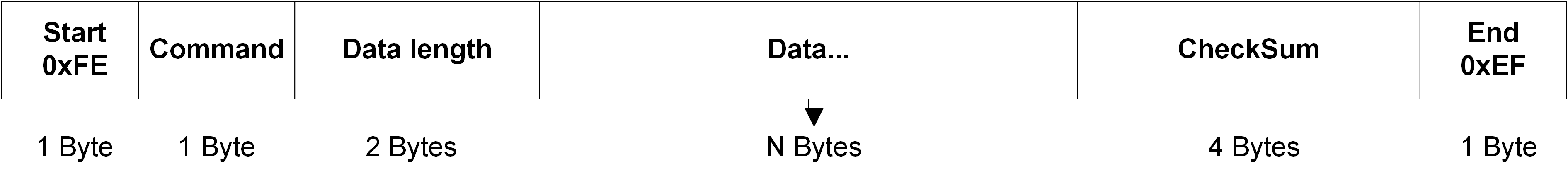
“Command” means the command id and the checksum algorithm is CRC32.
1.3.2 Response

“Status” means the status code, 0 means success, and non-0 value means failure. The checksum algorithm is CRC32.
1.4 Command Load Format
1.4.1 SYNC Command Load Format
Request:
None
Response:
None
1.4.2 JUMP Command Load Format
Request:
Addr: 4 Bytes, jump address
Response:
None
1.4.3 FLASH Command Load Format
Request:
Addr: 4 Bytes, download address
Size: 4 Bytes, download data length
Data: N Bytes, download data
Response:
None
1.4.4 ERASE Command Load Format
Request:
Addr: 4 Bytes, erasure address
Size: 4 Bytes, erasure area size
Response:
None
1.4.5 VERIFY Command Load Format
Request:
Addr: 4 Bytes, verification starting address
Size: 4 Bytes, verification area size
Checksum: 4 Bytes, verification checksum
Response:
None
1.4.6 WROTP Command Load Format
Request:
Addr: 4 Bytes, download address of OTP to write
Size: 4 Bytes, download data length
Data: N Bytes, download data
Response:
None
1.4.7 RDOTP Command Load Format
Request:
Addr: 4 Bytes, address of OTP to read
Size: 4 Bytes, data length
Response:
Data: N Bytes, data
1.4.8 WROPT0 Command Load Format
Request:
Opt0_l: 4 Bytes, lower 32 bits of Option0
Opt0_h: 4 Bytes, higher 32 bits of Option0
Response:
None
1.4.9 RDOPT0 Command Load Format
Request:
None
Response:
Opt0_l: 4 Bytes, lower 32 bits of Option0
Opt0_h: 4 Bytes, higher 32 bits of Option0
1.4.10 WROPT1 Command Load Format
Request:
Opt1_l: 4 Bytes, lower 32 bits of Option1
Opt1_h: 4 Bytes, higher 32 bits of Option1
Response:
None
1.4.11 RDOPT1 Command Load Format
Request:
None
Response:
Opt1_l: 4 Bytes, lower 32 bits of Option1
Opt1_h: 4 Bytes, higher 32 bits of Option1
1.4.12 REBOOT Command Load Format
Request:
None
Response:
None
1.4.13 SN Command Load Format
Request:
None
Response:
SN: 8 Bytes, serial number
1.4.14 WRREG Command Load Format
Request:
Addr: 4 Bytes, address of register to write
Value: 4 Bytes, value
Response:
None
1.4.15 RDREG Command Load Format
Request:
Addr: 4 Bytes, address of register to read
Response:
Value: 4 Bytes, value
1.4.16 BAUDRATE Command Load Format
Request:
Baudrate: 4 Bytes, baud rate
Response:
None
1.4.17 VERSION Command Load Format
Request:
None
Response:
Version: 4 Bytes, version number
2. Program for Reference
For the Bootloader communication program, please refer to build:raw-latex:scripts_loader.py.